






Ask a process engineer what causes a bad day on the line and masking tape rarely comes up. It is a consumable that costs cents per board. But the same tape is the only thing standing between a molten solder wave and a gold finger, between a conformal coating and a connector that must still mate, between an encapsulant and a sealing surface that has to stay clean.
When masking fails, it fails downstream: intermittent contact resistance, coating delamination, optical surfaces that drift out of spec weeks after final test. This article walks through eight real application scenarios in electronics manufacturing, which tape construction fits each one, and how to validate it before you commit.
The cases below describe typical process conditions. Run your own trial against your actual thermal profile and chemicals before locking a part number.
 First, a quick selection map
| Tape type | Typical backing | Temperature range | Best for | Watch out for |
|---|---|---|---|---|
| Crepe paper masking tape | Crepe paper, 0.11 mm | Room temp to ~120 °C | Conformal coating, packing, light holding, ESD-sensitive areas | Not for reflow; low elongation |
| PET / polyester tape | PET film | Up to ~150–180 °C | Plating, anodizing, general masking, spray paint | Can shrink at high heat |
| Polyimide (PI) tape, silicone adhesive | PI film, 0.025–0.06 mm | Up to 260–290 °C | Wave solder, reflow, high-temp shielding | Silicone transfer risk |
| Polyimide tape, non-silicone (acrylic) | PI film, 0.025 mm | 260 °C / 10 min | Optical modules, semiconductor packaging, anything bonded or coated after | Not automatically ESD-safe |
| Specialty (thermal release, UV release) | Film + functional adhesive | Process-specific | Wafer dicing, temporary bonding, clean debonding | Requires the trigger step |
The two variables that matter most are peak temperature with dwell time and what happens to the surface after removal. Everything else is optimization.
Case 1: Wave solder masking for gold fingers and edge connectors
The process. A through-hole board passes over a solder wave at roughly 250–260 °C. Gold fingers, edge connector lands and any area reserved for later bonding must stay solder-free.
The challenge. The tape has to survive immersion in flux, a preheat zone and direct solder contact without lifting at the edges. Lift means solder wicks underneath and the board is scrap. At the same time, the adhesive must not grab so hard that it leaves residue on the gold.
What works. A PI tape in the 0.06 mm range with a silicone adhesive rated to 290 °C, applied with firm roller pressure and burnished at the edges. IH803 (ESD PI tape, 0.06 mm, 290 °C) is built for this class of work, and the antistatic construction matters when the board carries unprotected components.
Validate by. Running a full wave profile, then inspecting the masked area for solder bleed, edge lift and adhesive residue under 10x magnification.
Case 2: Second-side reflow on double-sided SMT assemblies
The process. Board is reflowed, flipped, printed and reflowed again. Components already placed on side one pass back through the oven, and any exposed pads, sensors or connector windows on side two need protection.
The challenge. Two full thermal cycles with the tape already aged once. Adhesives that survive one pass often lift or leave residue on the second.
What works. A PI tape with stable adhesion after heat aging. If the board has optical windows, sensors or surfaces that will later be bonded or coated, specify a non-silicone construction such as IH890PN or IH890S rather than a silicone adhesive.
Validate by. Two complete reflow passes, then peel at the actual removal temperature (hot peel behaves differently from room-temperature peel) and check both the tape and the substrate.
Case 3: Conformal coating masking
The process. PCBA is coated with acrylic, urethane or silicone conformal coating. Connectors, test points, grounding pads and mating surfaces must stay clean.
The challenge. Coating is thin and creeps. Any gap at the tape edge produces a feathered coating line that flakes later. Just as important, peeling tape in a dry ESD-controlled area generates static.
What works. An anti-static crepe paper masking tape. E2-MA311 is a crepe-paper-based antistatic tape at 0.11 mm with 2–5 N/25 mm adhesion to steel, tensile strength above 2 kN/m, surface resistance of 10⁶–10¹¹ ohms and static discharge below 100 V on unwind. It is designed for clean removal without residue, which is what you want when the next station is a mating test.
| E2-MA311 property | Typical value |
|---|---|
| Total thickness | 0.11 ± 0.002 mm |
| Adhesion to steel | 2–5 N/25 mm |
| Tensile strength | ≥ 2 kN/m |
| Elongation | ≥ 5% |
| Surface resistance (backing / adhesive) | 10⁶–10¹¹ ohms |
| Static discharge | ≤ 100 V |
| Compliance | RoHS |
| Shelf life | 12 months (10–30 °C, 40–70% RH) |
Validate by. Coating, curing, then removing the tape and checking both the edge definition and whether the coating adhered where it was supposed to. A dyne test on the exposed surface catches silicone or adhesive transfer.
 Case 4: Dispensing, potting and UV adhesive damming
The process. Encapsulant or adhesive is dispensed into a housing. Adjacent areas, including lens seats, sealing grooves and connector bodies, must stay free of material.
The challenge. Low-viscosity encapsulant flows. The tape acts as a dam, so thickness and conformability matter as much as adhesion. Too thick and it changes the dispense geometry; too thin and material creeps under.
What works. A thin film tape with controlled thickness and good elongation, die-cut to the exact dam geometry. Where the encapsulant is UV-cured and the tape must release cleanly afterward, a UV release construction such as UV391PY removes the mechanical peel step entirely.
Validate by. Dispense, cure, then section the edge to measure how far material crept under the dam.
Case 5: Lithium battery cell and pack assembly
The process. Cells are stacked, insulated, welded and packed. Tabs, busbars and cell cans need temporary protection during welding and potting; separators and insulating plates need to be held in position.
The challenge. Metal dust from welding, electrolyte exposure, and strict insulation requirements between cells. Any conductive contamination between cells is a safety issue, not just a yield issue.
What works. For temporary masking around weld zones, a heat-resistant film tape that does not shed fibers. For permanent insulation and structural bonding inside the pack, die-cut double-sided foam or film tapes specified against the pack’s insulation and flame-retardancy requirements.Supplies die-cut battery plate parts in RoHS-compliant constructions.
Validate by. Welding with the tape in place, then checking for particle generation, adhesive softening and any change in the insulation resistance between adjacent cells.
Case 6: Resin bleed prevention in semiconductor and MEMS packaging
The process. Lead frames and substrate-based packages are encapsulated. Resin must fill the cavity and stay off the leads and sealing surfaces.
The challenge. Encapsulant is injected under pressure at elevated temperature. Any gap becomes a flash defect that requires deflash operations, and resin on a sealing surface ruins hermeticity.
What works. A high-temperature PI tape with stable adhesion and good tensile strength, applied as a dam. Silicone-free constructions are standard here because the leads will be plated or bonded afterward, and silicone residue blocks both.
Validate by. Mold, then inspect leads for flash under magnification and run a bond pull test on the exposed surface.
Case 7: Display modules, FPC handling and backing reinforcement
The process. Flex circuits, spacer films and thin substrates move between stations. They are too thin to handle bare, so they ride on a carrier.
The challenge. The carrier tape must hold during placement, survive any heating step, and release without stretching or leaving adhesive on a surface that will later be laminated or optically bonded.
What works. A film tape with high tensile strength and elongation, because the carrier sees mechanical stress, not just heat. For applications where optical bonding or lamination follows, use a non-silicone adhesive and confirm there is no transfer before the lamination step.
Validate by. Full handling cycle, then inspect the released surface under raking light for ghosting or adhesive haze.
Case 8: Optical module assembly, where silicone is disqualifying
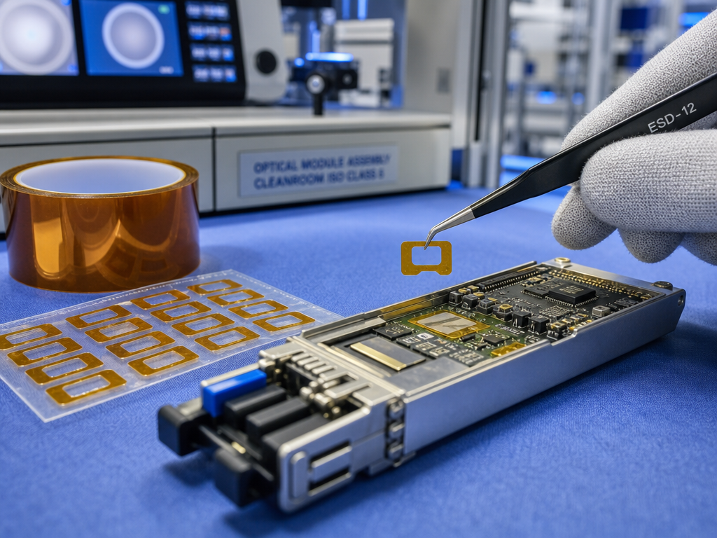
The process. TOSA/ROSA subassemblies, PCBA and fiber arrays are assembled, aligned and sealed. Masking and temporary fixation happen at several high-temperature stations.
The challenge. Low-molecular-weight siloxanes from a silicone adhesive volatilize under heat and redeposit as an invisible film. On a lens or fiber end-face, that film raises insertion loss and back-reflection. On a bond pad, it causes non-stick-on-pad events.
What works. A silicone-free PI tape. IH890PN uses a 0.025 mm PI film with an acrylic adhesive, total thickness 0.042 mm, 1.8–3.5 N/25 mm adhesion to steel, tensile strength above 3.5 kN/m, elongation above 45%, rated 260 °C for 10 minutes. It is specified for high-temperature shielding in packaging processes and removes without adhesive residue.
We covered this in detail in Silicone-Free High-Temperature Tape in Optical Module Manufacturing.
Validate by. Run the thermal profile, remove the tape, then perform the actual downstream bond or coupling step and measure. Silicone transfer problems only show up downstream, never at the tape removal station.
Failure modes and what they usually mean
| Symptom | Likely cause |
|---|---|
| Edge lift during heating | Adhesion too low, insufficient application pressure, or surface contamination |
| Adhesive residue after removal | Adhesion too high for the temperature, or removal too fast / at the wrong angle |
| Coating or epoxy won’t wet the surface | Silicone transfer, or adhesive residue invisible to the eye |
| Tape stretches and the part moves | Elongation too high or tensile strength too low for a fixturing application |
| Tape tears on removal | Elongation too low for curved or uneven surfaces |
| Unexplained ESD events at the station | Tape is not antistatic; check surface resistance and unwind voltage |
| Intermittent failures between lots | Adhesion or thickness varies lot to lot; ask for the control range |
How to qualify a masking tape in one week
- Write down the real profile. Peak temperature, dwell above 200 °C, number of passes, chemicals, and whether removal is hot or cold.
- Pick the station with the highest downstream sensitivity. If a tape fails there, it fails everywhere.
- Include the downstream operation in the trial. Remove the tape, then bond, coat, plate or couple, and measure the result.
- Remove at a controlled angle and speed. Slow, low-angle peeling reduces adhesive splitting after heat aging.
- Qualify two lots. Lot-to-lot variation is the most common cause of a process that used to work.
FAQ
Can I use crepe paper masking tape in a reflow oven?
No. Paper-based tape is generally limited to around 120 °C. Reflow needs a polyimide film tape.
Is a higher adhesion number better?
Not for masking. Above roughly 5 N/25 mm, residue risk climbs sharply after heat aging. For clean masking, 1.8–3.5 N/25 mm is a practical window.
Does anti-static tape replace other ESD controls?
No. It reduces charge generation at the tape itself, which matters on ESD-sensitive assemblies. It does not replace grounding, ionization or handling procedures.
What is the shelf life?
It varies by construction. E2-MA311 is 12 months from the date of manufacture in original packaging; non-silicone PI tapes such as IH890PN are typically 6 months. Store at 10–30 °C and 40–70% RH, away from direct sunlight.
Can tapes be die-cut to custom shapes?
Yes. Rolls, strips and liner-backed die-cut parts reduce manual trimming and improve placement repeatability. Provide the drawing, tolerances, liner requirements and delivery format.