





Gold fingers are the least forgiving surface on a PCB. A gold-plated edge connector has to survive storage, handling, one or more reflow passes, possibly a wave solder, coating, test and shipping, and then deliver a stable milliohm-level contact resistance when it is plugged in years later.
Almost nothing about that is forgiving of contamination. Flux residue, a fingerprint, a few nanometers of silicone, or a smear of adhesive left behind by masking tape will all show up as contact resistance drift or intermittent mated connection. And unlike a solder defect, contamination on a gold finger is invisible until it fails in the field.
This article covers six application cases where masking tape protects gold fingers, what each process demands from the tape, and how to choose and apply it.
What makes gold finger masking different
Three requirements separate gold finger masking from general PCB masking:
1. Zero residue, on a surface you cannot clean easily. Adhesive residue on a contact surface raises contact resistance. On fine-pitch connectors (0.5–1.0 mm pitch), even a thin film between the finger and the mating contact is a failure. Cleaning is possible but adds solvent handling, cycle time and its own contamination risk.
2. No edge lift, because bleed is worse than no mask. If the tape lifts at the edge during reflow, flux wicks underneath and contaminates the very area it was protecting. A partially masked gold finger is often worse than an unmasked one, because the residue sits exactly where the contact wipes.
3. Chemical compatibility with the process. Flux, cleaning solvents, plating chemistry or conformal coating — the tape has to sit in or next to these without breaking down.
Selection matrix
| Backing + adhesive | Peak temp | Multi-pass reflow | Residue behavior | Use for |
|---|---|---|---|---|
| PI + silicone adhesive | 260–290 °C | Yes, 4+ passes | Clean removal when cooled | Reflow, wave solder, standard SMT |
| PI + non-silicone (acrylic) | 260 °C / 10 min | Yes | Clean removal, no siloxane risk | Optical/connector fingers, anything bonded or coated later |
| PET + silicone | ~180–200 °C | 1–2 passes | Moderate | Coating masking, low-temp processes |
| Paper + rubber/acrylic | ~120 °C | No | Risk of carbonized deposit | Room-temperature holding and packing only |
A note on acrylic: general-purpose acrylic adhesives are not rated for lead-free reflow temperatures. High-temperature non-silicone constructions use a dedicated formulation and carry their own short-term rating — check the specific rating rather than assuming from the chemistry name.
Case 1: PCIe and DIMM gold fingers through lead-free reflow
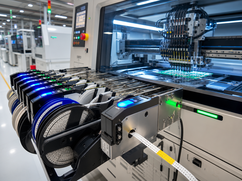
The process. A board with an edge connector — PCIe x1 to x16, DDR4/DDR5 DIMM, M.2, or an industrial backplane connector — goes through SAC305 reflow peaking at 245–260 °C. The gold fingers must come out of the oven clean.
The challenge. Multiple thermal passes on a double-sided assembly, tight pitch, and a contact surface that is evaluated on appearance and contact resistance. The tape also has to survive handling on a loaded board where components sit close to the board edge.
What works. A polyimide tape with stable adhesion across multiple passes and clean removal. For standard SMT, IH803 (ESD polyimide tape, 0.06 mm, rated to 290 °C) is the workhorse. Where an ESD-rated construction is required, and on populated boards it usually is, the antistatic backing matters at unwind, because the tape is peeled off right next to exposed devices.
Validate by. Full production profile, two passes minimum, then cool before removal and inspect the fingers under magnification. Measure contact resistance on a sample and compare against unmasked control boards.
Case 2: Wave solder on mixed-technology boards
The process. Through-hole components are soldered on a wave at 250–260 °C. The board passes over flux, preheat and molten solder. Any gold fingers on the board are directly exposed to all three.
The challenge. This is the harshest gold finger environment in SMT. Direct solder contact means any edge lift produces solder bridging between adjacent fingers, which is an immediate scrap. Flux immersion attacks the adhesive, and the thermal mass of the solder is far greater than convection reflow.
What works. A thicker polyimide tape, 0.06 mm rather than 0.025 mm, with high-temperature silicone adhesive, applied with firm roller pressure and the edges burnished down. The tape should extend past the finger zone onto the solder mask on all sides so the bond area sits on mask, not on gold.
Validate by. Full wave profile, then inspect for solder bridging, flux ingress under the tape, and adhesive residue. Do not hot peel; let the board cool first, because removing tape while the adhesive is soft and weakened leaves residue and can lift plating.
Case 3: Conformal coating and potting masking
The process. A board is conformal coated or potted. Connector fingers, test points and grounding pads must stay uncoated.
The challenge. Coating creeps. A gap at the tape edge produces a feathered film that either bridges onto the finger or flakes off later inside the connector. This process runs at room to moderate temperature, so the constraint is edge definition and static, not heat.
What works. An anti-static crepe paper tape. E2-MA311 is 0.11 mm with 2–5 N/25 mm adhesion, surface resistance of 10⁶–10¹¹ ohms and static discharge below 100 V on unwind, and it is specified for clean, residue-free removal. Paper is the right choice here: it conforms to board edges and, unlike film, does not create a hard step that coating can wick along.
Validate by. Coat, cure, remove, then check both the edge line and whether the coating bonded where intended. A dyne test on the exposed gold catches transfer that the eye will miss.
Case 4: Rework and selective soldering
The process. A component near the edge connector is replaced with a hot air rework station, or a selective soldering nozzle runs close to the finger area.
The challenge. Localized, uncontrolled temperature. A hot air nozzle pointed at a masked gold finger can exceed what the tape is rated for, and the operator usually cannot measure the actual temperature at the tape.
What works. Keep polyimide tape on the fingers and add a physical heat shield where a nozzle or hot air stream runs nearby. Use the highest-rated tape you stock for this station rather than the cheapest one, because the temperature excursion is unknown.
Validate by. Thermocouple the area during a representative rework cycle to find the real peak. Most rework residue complaints turn out to be over-temperature excursions, not tape defects.
Case 5: Optical modules and high-speed connectors — where silicone is disqualifying
The process. Optical transceiver and high-speed connector assemblies combine gold fingers with optical surfaces and fiber interfaces. Masking happens at several stations, often on the same fixture.
The challenge. A silicone adhesive releases low-molecular-weight siloxanes under heat. These volatilize, migrate and redeposit as an invisible film. On gold, that film raises contact resistance and blocks wetting if anything is soldered or bonded afterward. On an adjacent lens or fiber end-face, it raises insertion loss and back-reflection.
What works. A silicone-free polyimide tape. IH890PN pairs a 0.025 mm PI film with a specially formulated acrylic adhesive: total thickness 0.042 mm, 1.8–3.5 N/25 mm adhesion to steel, tensile strength above 3.5 kN/m, elongation above 45%, rated 260 °C for 10 minutes, with clean residue-free removal. IH890S covers applications needing a different adhesion balance.
We covered the contamination mechanism in detail in Silicone-Free High-Temperature Tape in Optical Module Manufacturing.
Validate by. Run the profile, remove the tape, then perform the downstream solder, bond or mating step and measure. Silicone transfer never shows up at the removal station — it shows up at the next one.
Case 6: PCB fabrication — HASL, plating and routing
The process. Before assembly ever happens, the bare board goes through surface finish and fabrication steps: HASL, ENIG, plating, and finally routing or V-cut depanelization.
The challenge. Plating baths and electrolytic chemistry, plus the mechanical abuse of routing dust and board handling. Tape used here must resist chemicals and stay attached through agitation.
What works. A polyimide tape with chemical resistance for the wet steps, and a robust film tape for routing protection on the finger area. Note that this is a different specification from SMT masking: chemical resistance and mechanical toughness matter more than removal cleanliness, because these tapes often come off before the board ships.
Validate by. Chemical immersion for the actual bath time and temperature, then check for edge lift, delamination and any change in the adhesive.
Sizing the tape correctly
Undersizing is the most common application error. Practical rules:
- Cover the finger zone plus margin. Extend the tape onto the solder mask by roughly 3 mm on each side so the primary bond area sits on mask rather than on gold.
- Wrap the board edge. For wave solder especially, fold the tape over the board edge so flux cannot enter from the side.
- Match width to pitch. On fine-pitch connectors, a tape that is too wide can overlap adjacent components; too narrow and it cannot cover the full finger length. Slits to custom widths and die-cuts to exact connector outlines, including notches and keying slots.
- Mind the step height. On 25 µm film, the tape edge is nearly flush and clears tight slot tolerances. Thicker film gives better tear resistance during manual application, at the cost of a larger step.
Application and removal: the six habits that prevent most defects
- Clean and dry the surface. Flux residue, fingerprint oil and moisture all reduce adhesion, and reduced adhesion means edge lift.
- Apply pressure. Roll or press the full area. Finger pressure leaves unbonded regions that lift during heating.
- Burnish the edges. The edge is where failure starts.
- Cool before removal. Removing while hot leaves residue and risks lifting plating.
- Peel slow and low. A slow pull at a low angle reduces adhesive splitting, especially after heat aging.
- Respect shelf life and storage. Non-silicone PI tapes are typically 6 months; E2-MA311 is 12 months. Store at 10–30 °C, 40–70% RH, out of direct sunlight.
Failure modes
| Symptom | Likely cause |
|---|---|
| Residue on the fingers | Adhesion too high for the profile, hot peel, or over-temperature excursion |
| Flux or solder under the tape | Edge lift from poor pressure, contamination, or tape too narrow |
| Contact resistance drift | Silicone transfer, or invisible adhesive film |
| Tape tears on removal | Film too thin for the handling, or overheated and embrittled |
| Coating or solder won’t wet the finger | Silicone contamination from an upstream tape |
| Discoloration or darkening of gold | Flux ingress or chemical attack through a lifted edge |
| ESD damage at the station | Non-antistatic tape; check surface resistance and unwind voltage |
FAQ
Can I use paper masking tape on gold fingers through reflow?
No. Paper-based tape is generally limited to about 120 °C and is not qualified for lead-free soldering. Use polyimide.
Should I remove the tape hot or cold?
Cold. Let the board return to room temperature. Hot adhesive is softened and much more likely to leave residue or lift plating.
Is silicone-free always better for gold fingers?
It is required when a bonding, coating, soldering or optical step follows, or when the assembly includes optical surfaces. For a straightforward reflow mask with no sensitive downstream step, a quality silicone PI tape performs well and costs less. Choose by process, not by principle.
Do I need ESD-rated tape?
If the board carries ESD-sensitive devices and the tape is peeled near them, yes. Standard polyimide tape generates charge on unwind.
What thickness should I use?
25 µm film for fine-pitch connectors where step height matters; 50 µm where tear resistance and handling robustness matter more, such as wave solder.
Can the tape be die-cut to my connector shape?
Yes. Custom slitting, die-cut pads matching the gold finger outline, and kiss-cut parts on liner for peel-and-place are all available.