

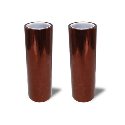
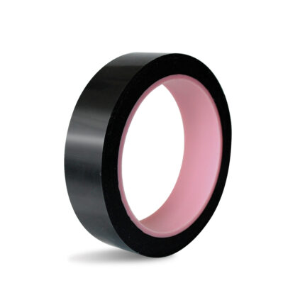






In most electronics assembly, tape is a consumable. In semiconductor packaging, it is closer to a process fixture. It is the material that determines whether a wafer survives back grinding down to 50 µm, whether dies stay put through a dicing blade spinning at tens of thousands of rpm, and whether a pick-and-place nozzle can lift a die cleanly off a film.
That role makes tape selection a yield decision rather than a purchasing decision. This article walks through seven application cases across the packaging flow, what each step demands, and how the release mechanism — UV, thermal or mechanical — should drive your choice.
The cases describe typical process conditions. Validate against your own recipe before qualifying a part number.
The release mechanism is the first decision
Every temporary tape in semiconductor packaging has to answer the same question: how does it let go? The answer determines which process steps it can serve.
| Type | Trigger | Before trigger | After trigger | Typical use |
|---|---|---|---|---|
| UV release tape | UV energy (dose + wavelength) | High adhesion, holds during cutting | Adhesion collapses near zero | Wafer grinding, dicing, expansion |
| Thermal release tape | Heat above a threshold | High initial tack | Adhesion disappears, auto-separation | Die sorting, temporary fixing, glass/ceramic dicing |
| Mechanical peel tape | Physical peel force | Moderate adhesion | Manual or automated removal | General masking, high-temp processes |
| High-temperature PI masking tape | Mechanical peel | Stable at 260–290 °C | Clean removal when cooled | Lead frame molding, die attach, wire bond |
The two programmable options, UV and thermal, exist because mechanical force is not acceptable on thin, brittle or expensive parts. Wherever a die, wafer or glass substrate could crack under peel stress, the release has to be triggered by energy rather than force.
Case 1: Wafer back grinding
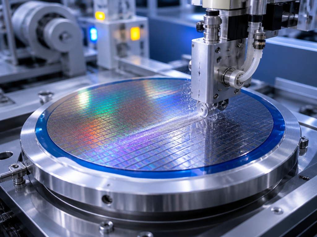
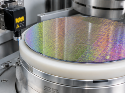
The process. After front-side processing is complete, the wafer is thinned from the back to reduce package height and improve thermal performance. The wafer is mounted face-down on a grinding tape, then ground, often followed by polishing or stress-relief etching.
The challenge. The tape absorbs grinding pressure and coolant while holding a wafer that gets progressively thinner and more fragile. It must be thick and compliant enough to cushion the device layer, uniform enough that total thickness variation stays inside spec, and adhesive-strong enough that no coolant or swarf penetrates under the edge. Then it has to release without leaving residue on an active surface.
What works. A UV release tape with high initial adhesion. KHJ’s UV396US is a single-sided UV debonding tape with high initial tack: 0.1 mm backing, 0.12 mm total thickness, 20 N/25 mm adhesion to steel before UV and 0.1 N/25 mm after, tensile strength 40 MPa, elongation 200%. Release condition is 500–600 mJ/cm² at a dominant wavelength of 365 nm.
Validate by. Grinding to target thickness, UV exposure at the specified dose, then checking for edge ingress, die lift during grinding, and residue after debonding. Confirm your UV lamp actually delivers the stated dose at the tape surface, because lamp aging is a common cause of inconsistent release.
Case 2: Wafer dicing and die expansion
The process. The thinned wafer on its film is mounted on a frame and cut into individual dies by a blade or laser. After dicing, the film is expanded to separate the dies, then exposed to UV so the dies can be picked.
The challenge. Two opposing requirements. During cutting, adhesion must be high enough that no die shifts, chips or flies off under blade force and coolant spray. After cutting, adhesion must be low enough that a pick-up needle and nozzle can release the die without cracking it or leaving adhesive on the back.
What works. The same UV release construction, with the dose tuned to the process. A drop from 20 N/25 mm to 0.1 N/25 mm is a large enough window to satisfy both ends. The film’s 200% elongation matters here too: it allows the expansion stage to stretch the film and open gaps between dies without the film tearing or over-thinning.
Validate by. Dicing, then inspecting chipping on the die sidewall, die displacement on the film, and pick-up success rate. Track the ratio of pick failures to UV dose — if it drifts, measure your lamp output before you change the tape.
Case 3: Die sorting, temporary fixing and transfer
The process. Dies, ceramic substrates, glass or metal plates are temporarily fixed for inspection, sorting, transfer or secondary processing, then released.
The challenge. Heat is often already part of the process, or easy to add. What is not acceptable is mechanical prying on thin or brittle parts, and the tape must not re-tack after release, or parts will stick again where they should not.
What works. A thermal release tape. KHJ’s TS600D is a blue thermal release tape with high initial tack: 0.1 mm backing, 0.155 ± 0.005 mm total thickness, 2–5 N/25 mm adhesion before heating and zero after, tensile strength above 3.5 kN/m, elongation above 120%. Adhesion disappears at 105–110 °C, and the recommended debonding process is 110 °C for 4–15 minutes depending on the heating method and how uniformly the attached object conducts and transfers heat. It will not re-tack after release.
Validate by. Heat the actual load, not just the plate. Thermal debonding failures are almost always uneven heat transfer, because a thick ceramic or glass part reaches the release temperature at its surface long before the adhesive layer does. Set the dwell from the slowest-heating point in the load.
Case 4: Lead frame molding and resin bleed control
The process. A lead frame or substrate strip is encapsulated by transfer molding. Resin fills the cavity and must not reach the leads, pads or sealing surfaces.
The challenge. Injection pressure and mold temperature around 175 °C. Any gap becomes flash, and resin on a lead or pad creates plating and bonding defects downstream.
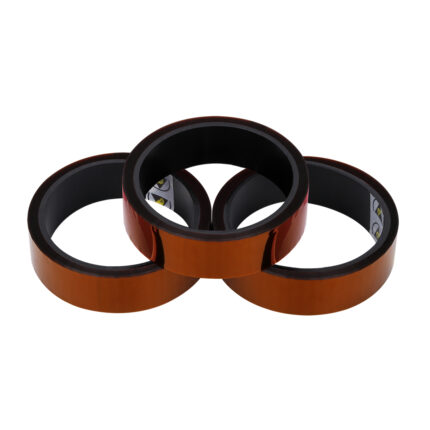
What works. A high-temperature polyimide masking tape as a dam, with stable adhesion and good tensile strength at temperature. Silicone-free constructions are standard in this step, because leads are plated and bonded afterward and silicone residue blocks both.
Validate by. Mold, then inspect leads for flash under magnification and run a bond pull test on surfaces that were masked.
Case 5: Die attach and wire bond — where silicone is disqualifying
The process. Die is attached to the substrate or lead frame, then wire bonded. Masking and temporary fixation happen around these steps.
The challenge. Silicone adhesives release low-molecular-weight siloxanes under heat. These volatilize, migrate and redeposit as an invisible film. On a bond pad, that film reduces wire pull strength and drives non-stick-on-pad (NSOP) events. On a die attach surface, it causes voids and delamination. This is why semiconductor lines specified silicone-free tape long before optical module makers did.
What works. A silicone-free polyimide tape. IH890PN pairs a 0.025 mm PI film with a specially formulated acrylic adhesive: 0.042 mm total thickness, 1.8–3.5 N/25 mm adhesion to steel, tensile strength above 3.5 kN/m, elongation above 45%, rated 260 °C for 10 minutes, clean residue-free removal. IH890S covers applications needing a different adhesion balance. UV391PY provides pre-cure adhesion with clean post-UV debonding where a UV trigger fits the line better than a peel.
Validate by. Run the thermal profile, remove the tape, then perform the actual die attach or wire bond and measure pull strength. Silicone transfer never appears at the removal station; it appears at the bonder.
Case 6: Glass, ceramic and metal substrate dicing
The process. Not everything on a packaging line is silicon. Glass interposers, ceramic substrates, MLCC blocks and metal plates are cut using the same equipment, and each needs a carrier.
The challenge. Different materials mean different surface energies, different thermal mass and different brittleness. A tape that releases cleanly from silicon may leave residue on glass, and a thermal release cycle tuned for silicon may not release a thick ceramic part on the same recipe.
What works. UV396US is specified for cutting and positioning protection of silicon crystals, glass, ceramic capacitors and PCBs. For heat-tolerant parts, TS600D gives a thermal alternative. Choose by material compatibility first, then by which trigger the line already has.
Validate by. Cut, release, then inspect the cut sidewall for chipping and the back surface for residue. Test each new substrate material separately; do not carry a recipe across materials.
Case 7: Advanced packaging and temporary bonding
The process. Fan-out wafer-level packaging, 2.5D/3D integration and TSV processes all need a wafer or panel temporarily bonded to a carrier so it can be thinned, processed on the back side and then released.
The challenge. The highest-value wafers in the fab, the tightest total thickness variation requirements, and a debond step where mechanical force is not an option. Thermal budget is also limited by what the device layer can tolerate.
What works. Programmable release films, UV or thermal depending on the carrier and the thermal budget. TS600D’s zero post-heat adhesion and no re-tack behavior suit debonding where parts must separate cleanly and stay separated. For panel-level processes, the film’s thickness uniformity and elongation determine how well it survives lamination and subsequent thermal steps.
Validate by. Full process simulation including lamination, thermal cycling and debond, checking for voids at the bond interface, thickness uniformity across the panel, and residue after release.
What to specify, beyond the datasheet
- Adhesion window, both ends. Pre-release adhesion must survive the process; post-release must be low enough for clean pick-up. Ask for both numbers, not just the “before” value.
- Trigger conditions, precisely. UV dose in mJ/cm² at a stated wavelength, or temperature plus dwell time. Verify your lamp output or your actual part temperature, not the equipment setpoint.
- Thickness and uniformity. Total thickness drives grinding TTV and package height. Tolerance matters more than nominal value.
- Elongation. Determines whether the film survives expansion and lamination without tearing.
- Residue and ionic content. Specify acceptance criteria. For devices, ask about ionic contamination and halide content explicitly.
- Silicone-free. Required wherever bonding, plating, coating or optical steps follow.
- Outgassing. For vacuum or sealed-cavity processes, state the test conditions and limits. Silicone-free is not the same as low-outgassing.
- Storage and shelf life. UV396US: 10–30 °C, 40–70% RH, dark and light-protected, 6 months. TS600D: same temperature and humidity, 12 months. UV tape exposed to ambient light loses performance long before the date on the label.
Failure modes
| Symptom | Likely cause |
|---|---|
| Dies shift or fly during dicing | Pre-release adhesion too low, or uneven application pressure |
| Pick-up failures after UV | UV dose below specification, or lamp output decayed |
| Residue after debonding | Under-exposure, over-exposure cross-linking, or expired tape |
| Film tears during expansion | Elongation insufficient, or expansion set beyond film capability |
| Uneven thermal release | Poor heat transfer uniformity; dwell set from plate temperature rather than part temperature |
| Parts re-stick after debonding | Tape not specified as no-re-tack |
| Wire bond NSOP or low pull strength | Silicone contamination from an upstream tape |
| Thickness variation out of spec | Film thickness tolerance, or lamination pressure issues |
FAQ
UV or thermal release — which should I use?
UV if you have a UV station and need fast, room-temperature release, and your parts are not UV-sensitive. Thermal if the part can tolerate 110 °C and you already have a heating step, or if the geometry blocks UV exposure. Many lines keep both.
What UV dose does UV396US need?
500–600 mJ/cm² at a dominant wavelength of 365 nm. Measure the dose at the tape surface rather than trusting the lamp setting.
What temperature does TS600D release at?
Adhesion disappears at 105–110 °C. The recommended debonding process is 110 °C for 4–15 minutes, with dwell depending on the heating method and the thermal conductivity and heat transfer uniformity of the attached object.
How long do these tapes keep?
UV396US is 6 months and must be stored dark and light-protected at 10–30 °C, 40–70% RH. TS600D is 12 months at the same temperature and humidity.
Does silicone-free mean low outgassing?
No. Silicone-free removes the siloxane risk. Low total outgassing is a separate specification and needs its own test conditions and limits.
Can these films be supplied in custom formats?
Yes. Rolls, sheets, custom widths and die-cut formats are available for frames and panel-level equipment.